
TECHNICAL BLOG
Analysing variations in Josephson junction barriers using a combined approach
- Extended electrical measurements are used to characterise Josephson junctions, probing the junction at voltages from zero, to the point where the junction permanently fails
- Combining electrical measurements and Monte-Carlo simulations shows that the thickness distribution of the Josephson junction oxide barrier likely has a non-normal probability distribution
- Testing with advanced microscopy shows that, while previously used to infer thickness distributions, Scanning Transmission Electron Microscopy can lose information about the true thickness distribution, introducing challenges with forming robust conclusions

Oscar Kennedy
HEAD OF DEVICE SCALING
Oscar has a background in quantum devices, RF instrumentation and materials science. Before joining OQC Oscar was a UCLQ fellow working on spin-based quantum memories. He now leads a team running projects spanning next generation sample packaging, superconducting device design and measurement.

Kevin Crawford
NANOFABRICATION ENGINEER
Kevin specialises in nanoscale electronics engineering and integrated circuit devices. He earned his PhD at the University of Glasgow, working in the James Watt Nanofabrication Centre. As a research associate there, and later a research fellow at the U.S. Army Research Laboratory, Sensors and Electron Devices Directorate, Kevin gained valuable fabrication experience in the use of novel materials for nanoscale device applications. His published work spans a range of topics, including wide bandgap semiconductors, atomic layer etching, field effect transistors, surface transfer doping, 2D materials, and quantum.

Kowsar Shahbazi
SENIOR NANOFABRICATION ENGINEER
Kowsar specialises in the design, fabrication, process development, and characterisation of devices, as well as deep look into the material science that goes behind the device performance. Prior to joining OQC, Kowsar served as a research associate at the University of Bath, and was a Marie Curie ESR in University of Leeds, where she oversaw the design, fabrication, and process optimisation of magnetic thin films and MEMS devices. Her expertise includes process design, nanofabrication, thin film systems, material science and metrology.

Connor Shelly
DIRECTOR OF MATERIALS SCIENCE & DEVICE ENGINEERING
As the Director of Materials Science and Device Engineering, Connor is responsible for the manufacturing of OQC’s qubits, QPUs, and superconducting devices, as well as being responsible for areas including qubit coherence, cryogenic packaging, materials science, and nanofabrication. Prior to joining OQC, Connor worked at the National Physical Laboratory (NPL) where he was the lead researcher for the Superconducting Electronics team and worked on the development of quantum limited amplifiers and carried out research into the physics of superconducting nanobridges as Josephson elements.
Josephson junctions, also known as JJs, are an enabling technology for quantum computing and hold significant technological importance. Precise manufacturing techniques are essential to the creation of tight tolerance JJs. However, in order to develop precise manufacturing techniques, a realistic understanding of the make-up of junctions is needed and robust feedback metrics are required to optimise manufacturing.
Optimisation of JJs manufacturing is an important element in quantum computing as this has been seen to affect how circuits operate during use, as reported in a recent Nature Physics paper where changes in qubit properties, like sensitivity to noise, have been linked to the atomic-scale structure of JJs.
What are Josephson junctions (JJs)?
The Josephson junction, predicted by British theoretical physicist Brian Josephson in 1962, consists of a thin non-superconducting layer between two superconducting layers. These junctions serve as the foundation for superconducting quantum circuits, they are the circuit element that provides the nonlinearity that is required to make a qubit.
The manufacturing process for JJs includes depositing an initial layer of aluminium which is then exposed to an oxygen environment so that the surface of the aluminium oxidises. Once the aluminium is coated with an oxide layer, it is capped with another layer of aluminium. A structure is therefore created where aluminium oxide is sandwiched between two layers of aluminium. When cooled to very low temperatures, the aluminium becomes a superconductor and the aluminium oxide remains an insulator, realising the superconductor-insulator-superconductor structure required to build JJs.
Why is barrier thickness important?
The properties of the JJs made with an aluminium oxide barrier layer depend very sensitively on the properties of the barrier layer. If the barrier is thin, it doesn’t isolate the two superconducting layers enough, and too thick of a barrier isolates the layers too strongly. In an ideal manufacturing process, we would have very precise control over the growth of this oxide layer. We typically find that the barrier is about 2 nm (nanometers) thick, and as the atomic radius of an oxygen ion is only around 0.14 nm, this means that the whole barrier will be ~10 atoms thick, and manufacturing on these length scales is challenging.
Characterising Josephson junctions
Two established techniques to characterise Josephson junctions are:
- measuring them electrically to find out their resistance at room temperature
- using advanced microscopy techniques where the Josephson junction is cut and the aluminium oxide is imaged
The Materials Science & Device Engineering team at OQC have considered and extended both of these techniques through in-depth analysis and simulation.
Electrical measurements
In a “normal” electrical measurement of a JJ at room temperature, a voltage would be ramped from a small negative value to a small positive value whilst the corresponding current flowing across the junction is measured. This dependence of the current flowing through the junction upon the voltage across the junction is called an “IV” . At low voltages the IV is linear, and Ohm’s law (V = IR) can be used to extract the resistance, this number is then used to characterise the JJ.
We intentionally ramp the voltage to a large enough value that the junction permanently fails (like a fuse blowing), which provides us with many useful pieces of information. We show an example of one of these IVs in Figure 1.
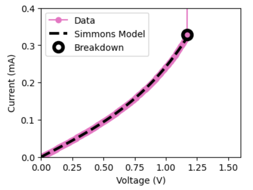
Figure 1. An example current-voltage relationship for a JJ measured at room temperature. We sweep the voltage whilst measuring the current until the junction spontaneously fails (at the point indicated by the circle). We can fit this with two models, a linear fit (or Ohm’s law) and the Simmons model which describes for tunnel currents through a barrier.
We can still use the low-voltage region of the IV to fit the junction resistance, however at higher voltages we see that the current no longer follows a linear dependence on voltage, as shown by the pink curve in Figure 1. We can therefore use a more complex equation to model our IV, which can capture the deviation, and gives us some additional information about our device.
Finally, we are able to record where the junction fails, as depicted by the black circle in Figure 1. Repeating this process on multiple junctions allows us to obtain statistical information characteristic of our manufacturing process, providing a much broader range of information than if only the resistance of each junction was measured.
Once sufficient data is collected, we start to build up computer models of JJs and validate them against the experimental data collected. In our computer model, we divide the junction up into many small pieces and treat each of them separately. We assign the thickness of each small piece according to a statistical model of thickness. This provides us with the ability to change the statistical models and review how well the model predicts the experimental data. When there is a good match between the model and the data, this provides evidence that the statistical model used predicted something correctly about the junction.
Key results found include:
- the probability distribution of the barrier thickness is likely skewed
- the potential barrier height is between 0.8 and 1.2 electron-volts
- weak points in the barrier that cause the junction to fail, also contribute to reducing the resistance of the junction
Electron microscopy
We utilised an advanced form of electron microscopy: Scanning Transmission Electron Microscopy (STEM), which allows for sub-nanometre resolution imaging of materials with elemental contrast. The technique can be applied to JJs where the barrier has been capped with a top electrode, i.e. after the full fabrication process has taken place. In academic literature this type of technique has previously been used to obtain the same type of information we produced in our computer modelling i.e. how much the thickness varies within a junction. In this section of our paper, we complete a deep-dive on this type of inference, attempting to ascertain how much trust should be placed on this type of inference.
Our key observation was that in STEM imaging, a 3D barrier is projected into a 2D image and in doing this information is lost about the true thickness distribution. The conclusion of our work was that, while the technique of transmission electron microscopy can be used to find average barrier thickness, there are challenges with forming robust conclusions from these experiments on the distribution of thicknesses in a barrier.
Read the full preprint on ArXiv
Analysis of Josephson Junction Barrier Variation — a Combined STEM, Breakdown and Monte-Carlo Approach.
Oscar W. Kennedy, Kevin G. Crawford, Kowsar Shahbazi, and Connor D. Shelly.
Join our newsletter for more articles like this
By clicking ‘sign up’ you’re confirming that you agree with our Terms & Conditions
