TECHNICAL BLOG
Overcoming the scale-up challenges of sapphire-based quantum processors
- In a world-first, we have developed a sapphire micro-machining process that integrates seamlessly with our intermediate-scale quantum processors.
- We have successfully demonstrated the process through the complete manufacturing process of our own 32-qubit OQC Toshiko QPU
- Our end-to-end process retains the high coherence qubits and the state-of-the-art wafer scale Josephson Junction spread to 2.5%, showing the process’s robustness.
- Our process mitigates low-frequency modes and allows a potential route through sapphire vias for the three-dimensional integration of superconducting qubit arrays.

Kowsar Shahbazi
SENIOR NANOFABRICATION ENGINEER
Kowsar specialises in the design, fabrication, process development, and characterisation of devices, as well as deep look into the material science that goes behind the device performance. Prior to joining OQC, Kowsar served as a research associate at the University of Bath, and was a Marie Curie ESR in University of Leeds, where she oversaw the design, fabrication, and process optimisation of magnetic thin films and MEMS devices. Her expertise includes process design, nanofabrication, thin film systems, material science and metrology.

Narendra Acharya
NANOFABRICATION ENGINEER
Narendra Acharya is a physicist specialising in superconducting device technology, nanofabrication, and metrology. He earned his PhD in Physics from Temple University, Philadelphia, where he conducted research on superconducting THz detectors for NASA’s Jet Propulsion Laboratory. After completing his doctorate, Narendra pursued a postdoctoral research fellowship at Chalmers University in Sweden, focusing on superconducting nanowire single-photon detectors. He is a nanofabrication engineer at Oxford Quantum Circuits (OQC), where he helps OQC to develop and fabricate quantum processors based on superconducting qubit technology.
Developing cutting-edge technology means we are continuously working to overcome challenges once thought impossible. However, on days like today, we (and the rest of our team!) get to celebrate as we publish breakthrough research that will not only encourage the advancement of superconducting qubit material platforms like tantalum on sapphire, but also provides the groundwork for exciting implications in scalability.
As superconducting qubit circuits become more complex, addressing a large array of qubits presents a significant engineering challenge. With the number of qubits growing, the physical dimensions of the quantum processor unit (QPU) increase, leading to frequency modes that are close or equal to the designed qubit frequencies.
Through-silicon vias (TSVs) have been proposed as a promising approach in superconducting qubit arrays to address this issue (Leek, P; Spring, P; 2019 Patent US11937517B2 and Peter A. Spring et al. Adv.8,eabl6698(2022)) TSVs can support densely packed qubit systems without compromising qubit performance or low-loss signal and control routing. Sapphire is a promising substrate for superconducting quantum processors due to its low-loss properties and proven high-coherence substrate platform for transmon qubits. The above mentioned scale-up engineering challenge remains the same for the sapphire platform and becomes even harder to solve, due to the difficulty of realising TSVs in sapphire compared to silicon substrates.
Why is scaling an issue?
As we make quantum processors bigger and more powerful, we also need to enlarge the package that they sit in – dimensions of the cavity housing the processors. But here’s the catch: bigger spaces mean lower resonance frequencies, and at some level the package supports frequencies that are the same as the designed qubit ones.
Essentially, as the enclosure becomes larger, these additional modes can disrupt the delicate quantum states of the qubits. This impacts the reliability and accuracy of the computations performed by the processor. Tackling this challenge, and other scaling issues, demands R&D efforts spanning hardware, error correction, control systems, algorithms, fabrication and materials. It’s a dedication required from our team, and teams across OQC.
Silicon vs. Sapphire: why does the choice of material matter?
While high-resistivity silicon has historically been the primary substrate material due to its compatibility with CMOS fabrication and simplicity of through-substrate holes and vias (electrical connection through holes), sapphire is a very real, if not better, alternative in superconducting circuits. Sapphire, as a dielectric substrate, offers low-loss properties, and high-coherence qubits was successfully demonstrated on it, extending qubit lifetimes to over 0.4 ms; one of the highest coherence times ever shown for superconducting qubits.
However, sapphire presents very real challenges in the context of superconducting circuits:
1) Firstly, sapphire is chemically inert, which means it does not easily react with most chemicals. This makes it a durable material but many standard etching processes, such as dry etch or wet etch used in micromachining and device fabrication are ineffective.
2) Secondly, sapphire is one of the hardest materials. Sapphire’s low fracture toughness makes it prone to cracking or chipping during machining processes, especially when creating precise features like apertures required for our QPU fabrication process.
To add more to the complexity, the choice of point in the end-to-end process that machining occurs also matters. Whether it is done at the start or middle of the process, the presence of holes in the substrate makes fabrication of Josephson junctions very challenging resulting in low yield. Also, the type of machining used needs careful consideration. For example, during machining processes like laser drilling, sapphire can experience significant heating that can be detrimental to the delicate components of superconducting circuits.
Overall, while sapphire offers advantages such as low loss tangents, its inherent hardness, and limited machinability pose very real challenges in fabricating ever bigger superconducting circuits. That is until today…
Micro-machining as an alternative to etching
Multiple approaches were tested such as laser drilling in addition to researching the point at which aperture drilling was included in the process flow. These learning helped point us in the direction of micromachining.
Micro-machining refers to the precise removal of material to create small, intricate structures. This process can involve various methods, such as etching, laser cutting, or mechanical milling, to shape the substrate at micro scales. This technology is common for fabricating MEMS devices, semiconductor components, and photonic circuits..
The process involved protecting the circuit with several layers of different coatings, and actively cooling the substrate during drilling to prevent damage to the substrate and nanofabricated circuits. We also determined that if machining occurs after the fabrication of Josephson junctions (JJs), it will minimise the risk of damage.
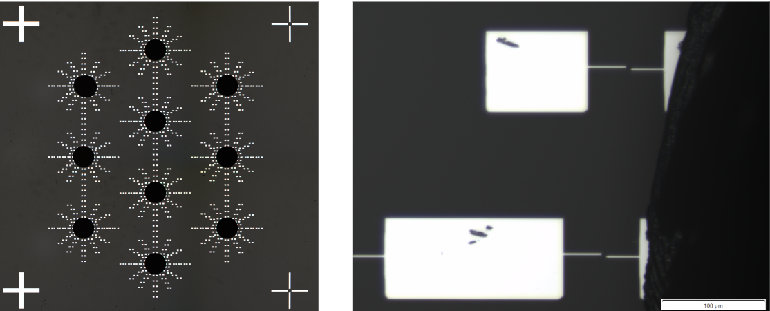
Fabricating JJs in a radial pattern, we have checked the safe distance of circuit components to micro machined apertures. Even JJs as close as 50 µm (same thickness as a human hair) to the aperture edge survived. Not only does this demonstrate how robust our junctions are, but it clearly demonstrates that this drilling technique is working for us.

Left: Josephson junctions fabricated in radial pattern around where it was going to be micro-machined later. Right: JJs located <100 micrometre away from the drilling edge were measured and found to be functional. Considering the difficulty of successfully getting a proper connection from an approx 15 micrometre sized probe on such a small area of the remaining contact pad it is remarkable that the JJs worked when so close to a machining process and all that it entails.
This technique not only facilitates the scaling of quantum processors but also paves the way for the development of through-sapphire-vias. These vias can be essential for leveraging the low-loss dielectric properties of sapphire in large-scale QPUs. This advancement was demonstrated through the complete manufacturing process of our own 32-qubit OQC Toshiko QPU, which is integrated with through-sapphire machining for mode-mitigation purposes. With an end to end process, we could still achieve a 2.5% room temperature resistance spread, which is in-line with the state-of-the-art wafer scale JJ fabrication spread values, without any machining!
Ultimately, our goal is to streamline fabrication, minimising mechanical disturbances and yielding cleaner devices for improved performance. And, the best part of it all is playing at the cutting edge: we have done something new – and we’ve done it as a team.
We have demonstrated a sapphire machining process compatible with high-coherence qubits, addressing the existing limitations, ultimately paving the way for widespread adoption in the field.
Integration of through-sapphire substrate machining with superconducting quantum processors.
Narendra Acharya, Robert Armstrong, Yashwanth Balaji, Kevin G. Crawford, James C. Gates, Paul C. Gow, Oscar W. Kennedy, Renuka Devi Pothuraju, Kowsar Shahbazi, and Connor D. Shelly.
Join our newsletter for more articles like this
By clicking ‘sign up’ you’re confirming that you agree with our Terms & Conditions


